- 您现在的位置:买卖IC网 > Sheet目录694 > MAX17410GTM+ (Maxim Integrated)IC CTLR QPWM 2PH FOR IMV 48TQFN
�� �
�
�Dual-Phase,� Quick-PWM� Controller�
�for� IMVP6+� CPU� Core� Power� Supplies�
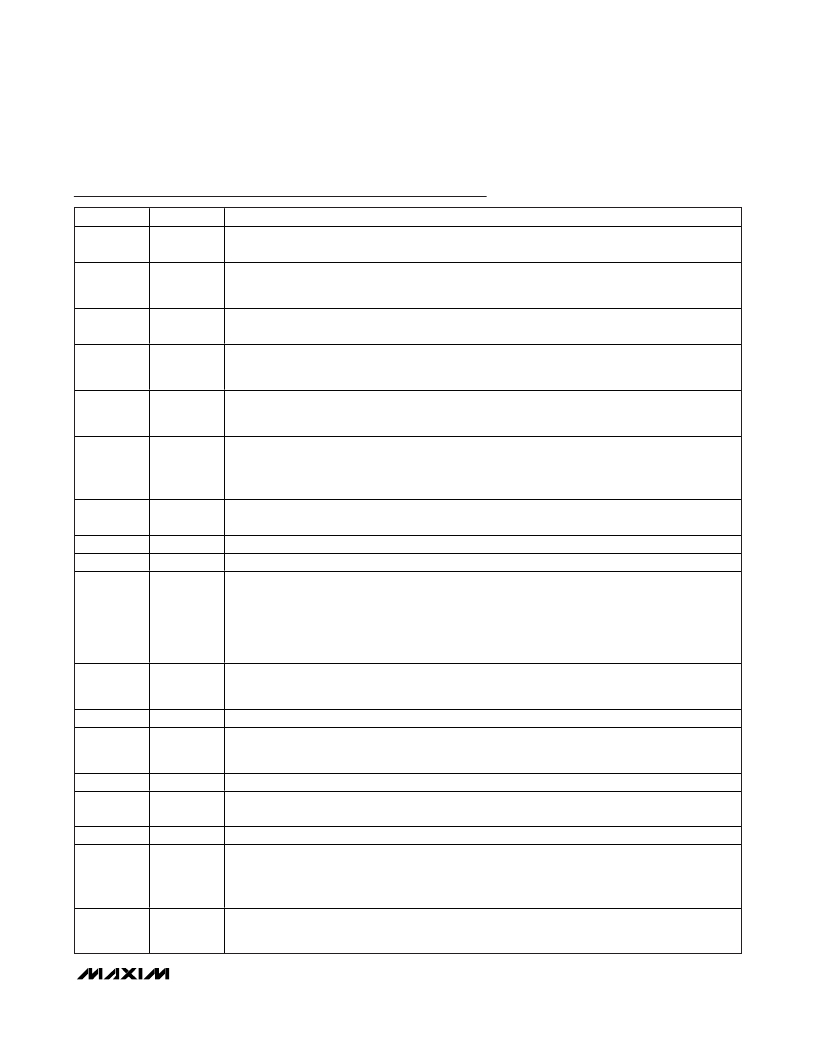
�Pin� Description� (continued)�
�PIN�
�NAME�
�FUNCTION�
�14�
�OUTS�
�Output� Remote� Sense.� Internally� shorted� to� VPS� through� a� 10�
�voltage� feedback� input� to� the� power� monitor.�
�resistance.� OUTS� is� also� the�
�Feedback� Remote-Sense� Input,� Negative� Side.� Normally� connected� to� GND� directly� at� the� load.�
�15�
�16�
�17�
�18�
�19�
�20�
�21�
�22�
�23�
�24�
�25�
�26�
�27�
�28�
�29�
�30�
�31�
�GNDS�
�CCI�
�CSN2�
�CSN1�
�CSPAVG�
�IN�
�GND�
�V� CC�
�CSP2�
�CSP1�
�N.C.�
�BST2�
�DH2�
�LX2�
�PGND2�
�DL2�
�V� DD�
�GNDS� internally� connects� to� a� transconductance� amplifier� that� fine� tunes� the� output� voltage—�
�compensating� for� voltage� drops� from� the� regulator� ground� to� the� load� ground.�
�Current-Balance Compensation. Connect a 470pF capacitor between CCI and the positive side of the�
�feedback� remote-sense� input� (or� between� CCI� and� GND).� CCI� is� internally� forced� low� in� shutdown.�
�Negative� Input� of� the� Output� Current� Sense� of� Phase� 2.� This� pin� should� be� connected� to� the�
�negative side of the output current-sensing resistor or the filtering capacitor if the DC resistance of�
�the� output� inductor� is� utilized� for� current� sensing.�
�Negative� Input� of� the� Output� Current� Sense� of� Phase� 1.� This� pin� should� be� connected� to� the�
�negative side of the output current-sensing resistor or the filtering capacitor if the DC resistance of�
�the� output� inductor� is� utilized� for� current� sensing.�
�Positive� Input� of� the� Output� Current-Sense� Averaging� Network.� This� input� should� be� connected� to� the�
�positive� current-sense� averaging� network� (see� the� standard� 2-phase� IMVP6+� application� circuit� of�
�Figure� 1)� and� is� utilized� for� load� line� control� and� power� monitoring� (input� of� the� transconductance�
�amplifiers� used� for� FB� and� PMON).�
�Input Sense for On-Time Control. An internal resistor sets the switching frequency to 300kHz per�
�phase.� IN� is� high� impedance� in� shutdown.�
�Analog� Ground� Connect�
�Controller� Supply� Voltage.� Connect� to� a� 4.5V� to� 5.5V� source.� Bypass� to� GND� with� 1� μF� minimum.�
�Positive� Input� of� the� Output� Current� Sense� of� Phase� 2.� This� pin� should� be� connected� to� the� positive�
�side of the output current-sensing resistor, or to the filtering capacitor if the DC resistance of the output�
�inductor� is� used� for� current� sensing.� This� pin� is� utilized� for� current� limit� and� current� balance� only.�
�Connect CSP2 to V� CC� to disable phase 2 and use the MAX17410 as a single-phase controller. In�
�this configuration, connect LX2 to GND, connect BST2 to V� DD� , CSN2 to CSN1, and float DH2, DL2,�
�CCI,� and� PHASEGD.�
�Positive� Input� of� the� Output� Current� Sense� of� Phase� 1.� This� pin� should� be� connected� to� the� positive�
�side of the output current-sensing resistor, or to the filtering capacitor if the DC resistance of the output�
�inductor� is� used� for� current� sensing.� This� pin� is� utilized� for� current� limit� and� current� balance� only.�
�No� Connection.� Not� internally� connected.�
�Phase� 2� Boost� Flying� Capacitor� Connection.� BST2� is� the� internal� upper� supply� rail� for� the� DH2�
�high-side� gate� driver.� An� internal� switch� between� V� DD� and� BST2� charges� the� BST2� -� LX2� flying�
�capacitor� while� the� low-side� MOSFET� is� on� (DL2� pulled� high).�
�Phase� 2� High-Side� Gate-Driver� Output.� DH2� swings� from� LX2� to� BST2.� Low� in� shutdown.�
�Phase 2 Inductor Connection. LX2 is the internal lower supply rail for the DH2 high-side gate driver.�
�Also� used� as� an� input� to� phase� 2� ’s� zero-crossing� comparator.�
�Power� Ground.� PGND2� is� the� internal� lower� supply� rail� for� the� DL2� low-side� gate� driver.�
�Phase� 2� Low-Side� Gate-Driver� Output.� DL2� swings� from� PGND2� to� V� DD� .� DL2� is� forced� low� in�
�shutdown. DL2 is forced high when an output overvoltage fault is detected, overriding any�
�negative� current-limit� condition� that� might� be� present.� DL2� is� forced� low� in� skip� mode� after�
�detecting� an� inductor� current� zero� crossing.�
�Supply Voltage Input for the DL_ Drivers. V� DD� is also the supply voltage used to internally recharge�
�the BST_ - LX_ flying capacitor during the times the respective DL_ are high. Connect V� DD� to the�
�4.5V to 5.5V system supply voltage. Bypass V� DD� to GND with a 1μF or greater ceramic capacitor.�
�______________________________________________________________________________________�
�17�
�发布紧急采购,3分钟左右您将得到回复。
相关PDF资料
MC2711H
SWITCH BUSHING PLUNGER W/SEAL
MC2711
SWITCH BUSHING MOUNT PLUNGER
MC7711
SWITCH BUSHING MOUNT PLUNGER
MCA7711
SWITCH BUSHING MOUNT PLUNGER
MCD2711
SWITCH BUSHING MOUNT PLUNGER
MCD7711
SWITCH BUSHING MOUNT PLUNGER
MCZ2010AH900
CHOKE COMMON MODE 90 OHM SMD
MCZ2010CH240L4T
CHOKE COMMON MODE 24 OHM SMD
相关代理商/技术参数
MAX17410GTM+T
功能描述:电流型 PWM 控制器 NDA IC RoHS:否 制造商:Texas Instruments 开关频率:27 KHz 上升时间: 下降时间: 工作电源电压:6 V to 15 V 工作电源电流:1.5 mA 输出端数量:1 最大工作温度:+ 105 C 安装风格:SMD/SMT 封装 / 箱体:TSSOP-14
MAX17411GTM+
功能描述:电流型 PWM 控制器 IMVP7 CPU & Graphics Controller RoHS:否 制造商:Texas Instruments 开关频率:27 KHz 上升时间: 下降时间: 工作电源电压:6 V to 15 V 工作电源电流:1.5 mA 输出端数量:1 最大工作温度:+ 105 C 安装风格:SMD/SMT 封装 / 箱体:TSSOP-14
MAX17411GTM+T
功能描述:电流型 PWM 控制器 IMVP7 CPU & Graphics Controller RoHS:否 制造商:Texas Instruments 开关频率:27 KHz 上升时间: 下降时间: 工作电源电压:6 V to 15 V 工作电源电流:1.5 mA 输出端数量:1 最大工作温度:+ 105 C 安装风格:SMD/SMT 封装 / 箱体:TSSOP-14
MAX17411RGTM+
功能描述:电流型 PWM 控制器 RoHS:否 制造商:Texas Instruments 开关频率:27 KHz 上升时间: 下降时间: 工作电源电压:6 V to 15 V 工作电源电流:1.5 mA 输出端数量:1 最大工作温度:+ 105 C 安装风格:SMD/SMT 封装 / 箱体:TSSOP-14
MAX17411RGTM+T
功能描述:电流型 PWM 控制器 RoHS:否 制造商:Texas Instruments 开关频率:27 KHz 上升时间: 下降时间: 工作电源电压:6 V to 15 V 工作电源电流:1.5 mA 输出端数量:1 最大工作温度:+ 105 C 安装风格:SMD/SMT 封装 / 箱体:TSSOP-14
MAX17411RGTM+TW
功能描述:电流型 PWM 控制器 RoHS:否 制造商:Texas Instruments 开关频率:27 KHz 上升时间: 下降时间: 工作电源电压:6 V to 15 V 工作电源电流:1.5 mA 输出端数量:1 最大工作温度:+ 105 C 安装风格:SMD/SMT 封装 / 箱体:TSSOP-14
MAX17411RGTM+W
功能描述:电流型 PWM 控制器 RoHS:否 制造商:Texas Instruments 开关频率:27 KHz 上升时间: 下降时间: 工作电源电压:6 V to 15 V 工作电源电流:1.5 mA 输出端数量:1 最大工作温度:+ 105 C 安装风格:SMD/SMT 封装 / 箱体:TSSOP-14
MAX17412ETI+
制造商:Rochester Electronics LLC 功能描述: 制造商:Maxim Integrated Products 功能描述: